8-bit Computer Clock - Page 1
Parts of the Circuit
I will need this clock circuit to be flexible enough to allow me to develop and fault find the computer. It needs to produce an adjustable clock pulse so I can slow down or speed up the computers operation. It will also need a manual pulse option so I can step through the computers operation one pulse at a time for fault finding. I will also include a software controllable halt option, and an inverted clock signal output. The adjustable clock will run at a maximum of about 500Hz, though I will also make it possible to switch over to a 5Mhz clock pulse so I can ramp the computer up to do more interesting stuff later on.
I'm designing the circuit using LTspice.
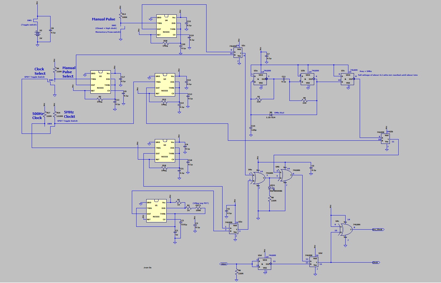
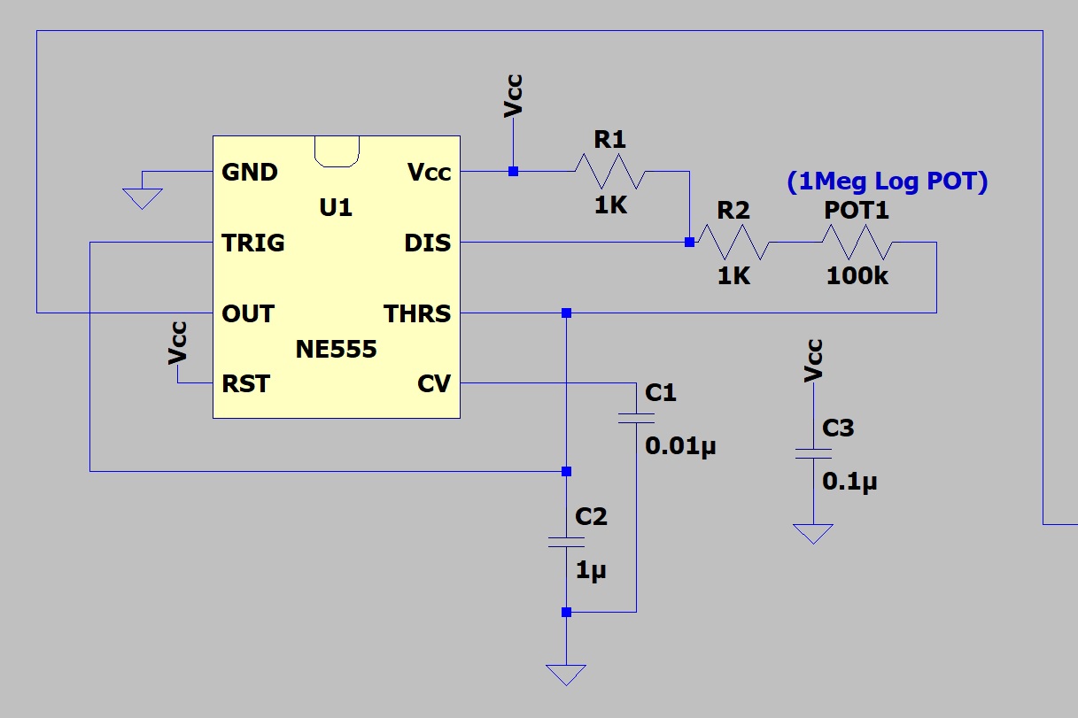
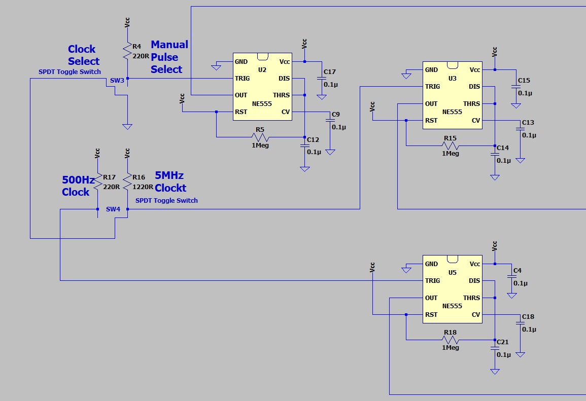
500Hz Adjustable Clock
The 500Hz clock pulse is created using the 555 timer circuit below. The frequency is adjusted using a 1Meg pot 'POT1'. The clock should have a range of 0.6 Hz to 500Hz, which is about 1 pulse every 1.5 seconds to 1 pulse every 2 ms.
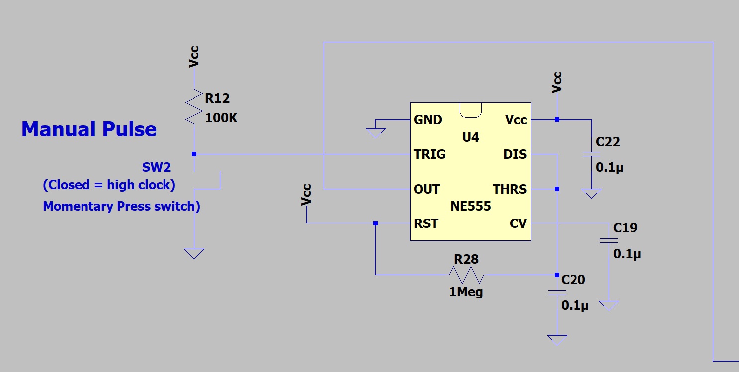
Manual Clock Pulse
The manual clock pulse is generated using a momentary press button switch. This triggers a 555 timer pulse circuit so that any switch bounce is eliminated. The 555 circuit will pulse no more than once about every 110ms no mater how many input pulses it receives.
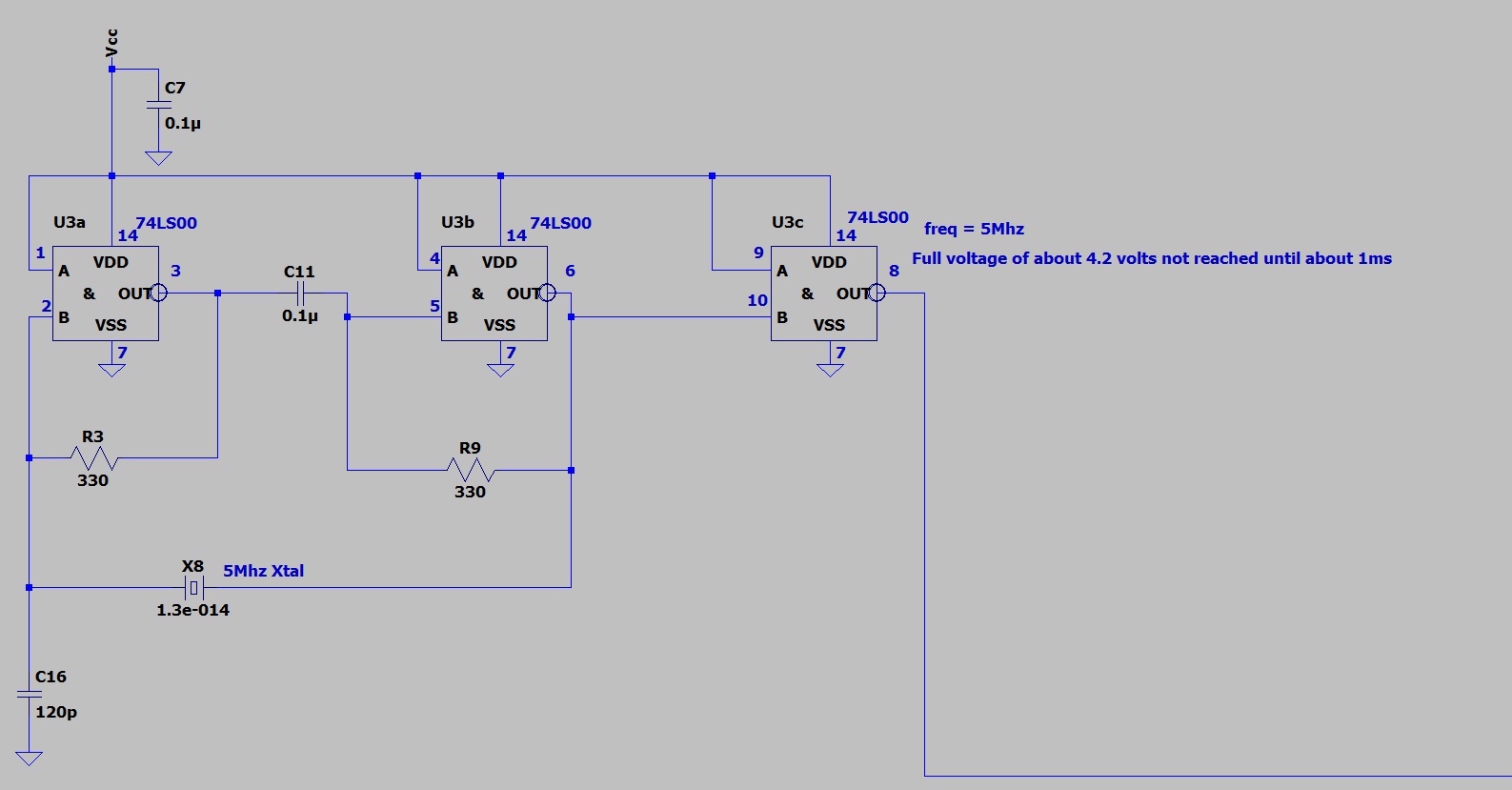
The 5MHz Clock
The 5MHz clock pulse is achieved separately as shown in fig 3, using 3 NAND gates and a 5MHz crystal. For this I used the 74LS00 IC which contains 4 2-input NAND Gates.
Clock Selection Circuit
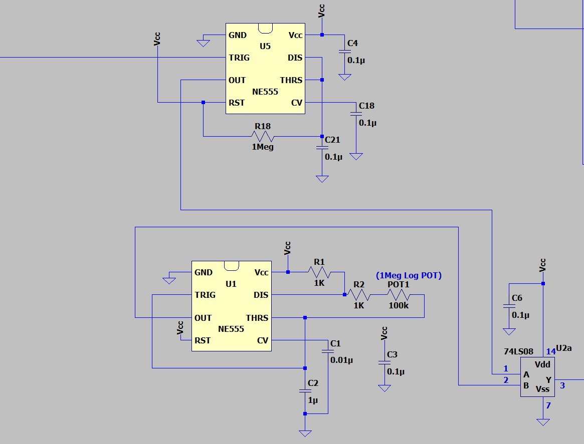
Two SPDT toggle switches are used. One to choose between Manual and Clock Pulse, and one to choose between the 500Hz clock and the 5MHz clock. The three possible choices go through three 555 debounce circuits. A low on the Trig pin of each 555 chip will give a high output, and vice versa
Each of which then goes to a 74LS08 AND gate as shown below. As long as either of the 2 inputs of a AND gate are low the output will be low, both inputs need to be high to get a high output. Therefore the AND gates in the two circuits that are not selected will have low outputs from the 555 out pins, and only the selected circuit will have a high on the out pin. Therefore when the clock pulse is high on the selected circuit the AND gate will have 2 high inputs and so a high output.
So that I don't tie them all together directly the outputs of the 3 AND gates go through a couple of 74LS86 Exclusive-OR Gates. The Manual and 500Hz clocks both go through the first Exclusive-OR Gate, which I placed an LED on the output of to flash when the signal is high. This signal then goes through the second Exclusive-OR Gate along with the 5MHz signal. There is no point having an LED on the 5MHz clock for obvious reasons.
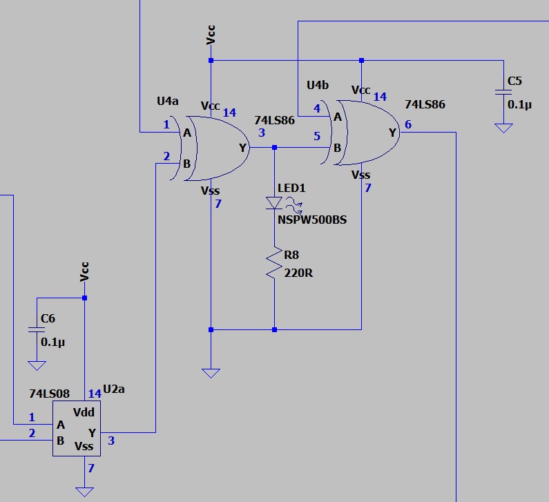
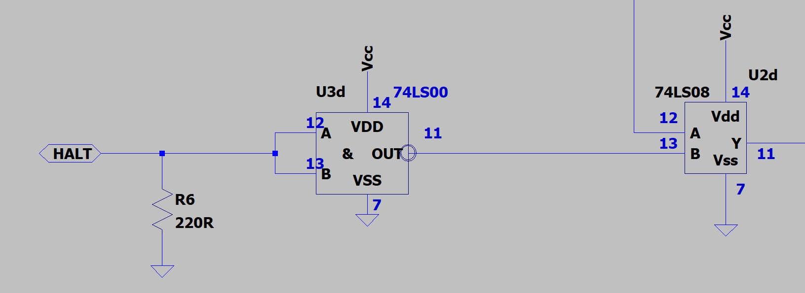
Halt Clock Circuit
There was one NAND gate left over from the 74LS00 chip I used for the 5MHz clock, so I used that as an inverter to make the Halt controle active on a high input. I used the last remaining AND gate from the 74LS08 chip to block the clock signal if the output from the inverter goes low.
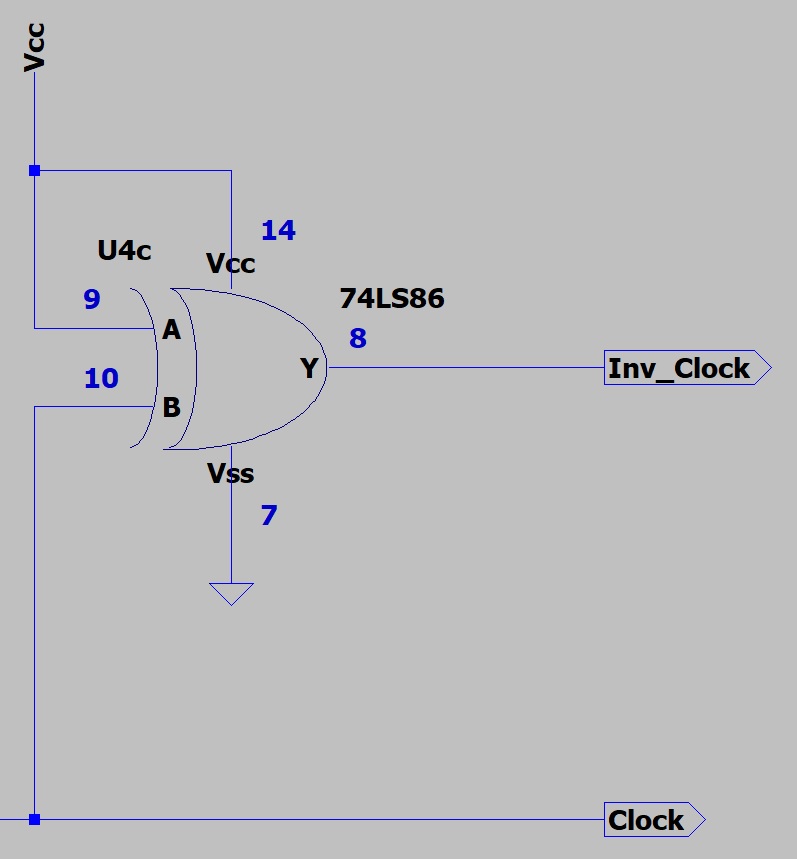
Inverted Clock
I used one of the 2 remaining Exclusive-OR Gates in the 74LS86 chip as an inverter to create an inverted clock output.
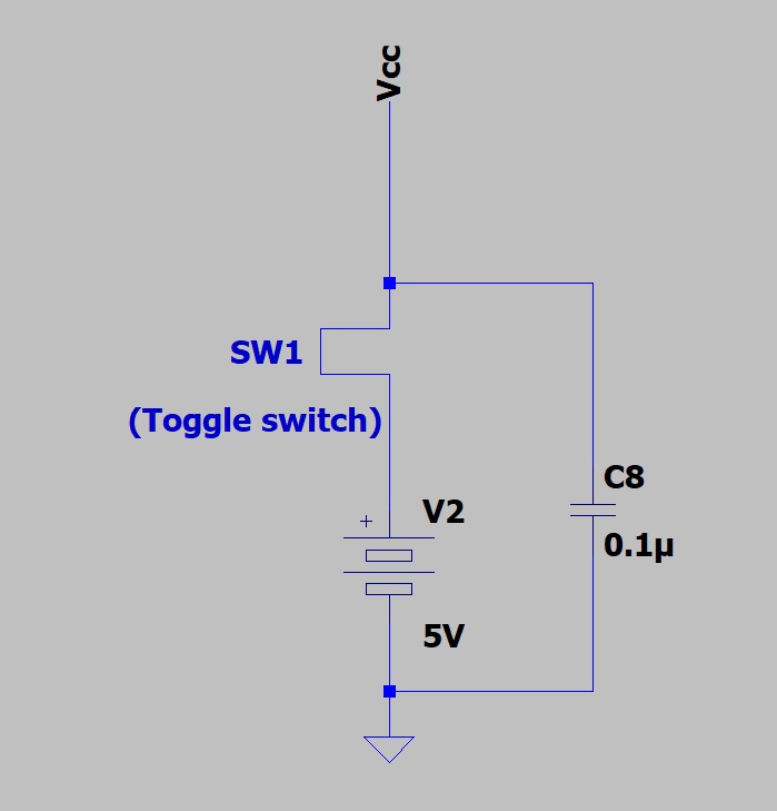
Power
The power is 5 volts supplied from a USB input. I also added bypass capacitors on all the IC's as well as across the supply voltage.